
The ability to handle turn-key projects at any given time with professional and technical proficiency.


Single Side PCBs
Single-sided PCBs, as their name suggests, have only one layer of conductive material. This makes them simple to design and manufacture. The process involves laminating one thin layer of thermally conductive and electrically insulating dielectric material with copper. Initially, PCBs were made manually, but with advancements in technology, they can now be designed using PCB design software such as ORCAD, EAGLE, PROTEL, and KICAD. The process begins with designing the PCB on a computer and printing or plotting it on film. The image is then transferred onto a PCB sheet through screen printing, followed by the etching process, which dissolves the copper except for the printed layer. Solder mask and Legend are then printed on the sheet, and holes are drilled for inserting components. Single-sided PCBs are ideal for simple designs and are widely used in consumer electronic products, digital cameras, audio amplifiers, power supplies, and switching relays.
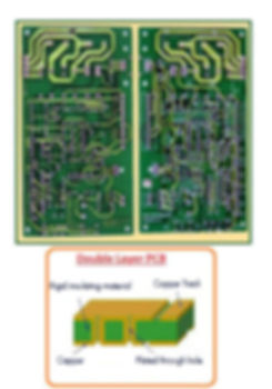
Double Side PCBs
Double sided PCBs are a type of printed circuit board that have conductive material on both sides of the board. They consist of a thin insulating layer (dielectric material) sandwiched between two layers of conductive material, usually copper, that are then laminated together. The conductive layers are connected through plated-through holes, which allow the components to be mounted on both sides of the board and interconnected as needed. This design allows for more complex circuitry and a higher density of components than single sided PCBs, making them suitable for a wider range of electronic applications. Double sided PCBs are commonly used in a variety of electronic devices, including computers, telecommunications equipment, medical equipment, and automotive electronics, among others.

Multi-layer PCBs
Multi-layer PCBs are a type of printed circuit board that has more than two layers of conductive material separated by insulating layers. They consist of multiple layers of conductive material, typically copper, that are separated by insulating layers made of a dielectric material such as fiberglass or plastic. The layers are then laminated together to form a single board with multiple layers of conductive material interconnected by plated-through holes. This design allows for a higher density of components and more complex circuitry than single or double sided PCBs, as well as better electrical performance and signal integrity. Multi-layer PCBs are commonly used in high-performance electronic devices, including computer motherboards, servers, networking equipment, and high-end consumer electronics such as smartphones and tablets. They are also used in aerospace and military applications, where reliability and performance are critical. Multi-layer PCBs can be more expensive and complex to design and manufacture than single or double sided PCBs, but their benefits in terms of performance and functionality make them a preferred choice for many electronic applications.

Metal Core PCBs
Metal Core PCBs (MCPCBs) are a type of printed circuit board that has a metal core, typically made of aluminum or copper, instead of an insulating material. The metal core acts as a heat sink, dissipating heat generated by the components on the board, which can be particularly useful in high-power or high-temperature applications. The metal core is typically coated with a thin layer of dielectric material, such as epoxy or polyimide, on which the circuitry is printed. The circuitry is then covered with a layer of solder mask and a layer of silkscreen to provide component placement and identification. MCPCBs are commonly used in high-power LED lighting, automotive electronics, power supplies, and other high-temperature applications where efficient heat dissipation is critical. They offer several advantages over traditional PCBs, including improved thermal management, increased mechanical strength, and reduced risk of component failure due to overheating. However, MCPCBs can be more expensive and difficult to manufacture than traditional PCBs due to the added complexity of the metal core.